Every electronic designer may need a simple mechanical integration into a housing or only some protective shields for his electronic assembly.
In my opinion the most critical point is, when some connectors have to be soldered directly onto the PCB or if they are mounted into the case walls and reaching far into the housing. In this case, some simple 3D PCB Information is sufficient to see if there are collisions, and if the whole assembly group fits into the housing. Well, this check may be part of the mechanical designer, but to ease this step 3D PCB Data is required.
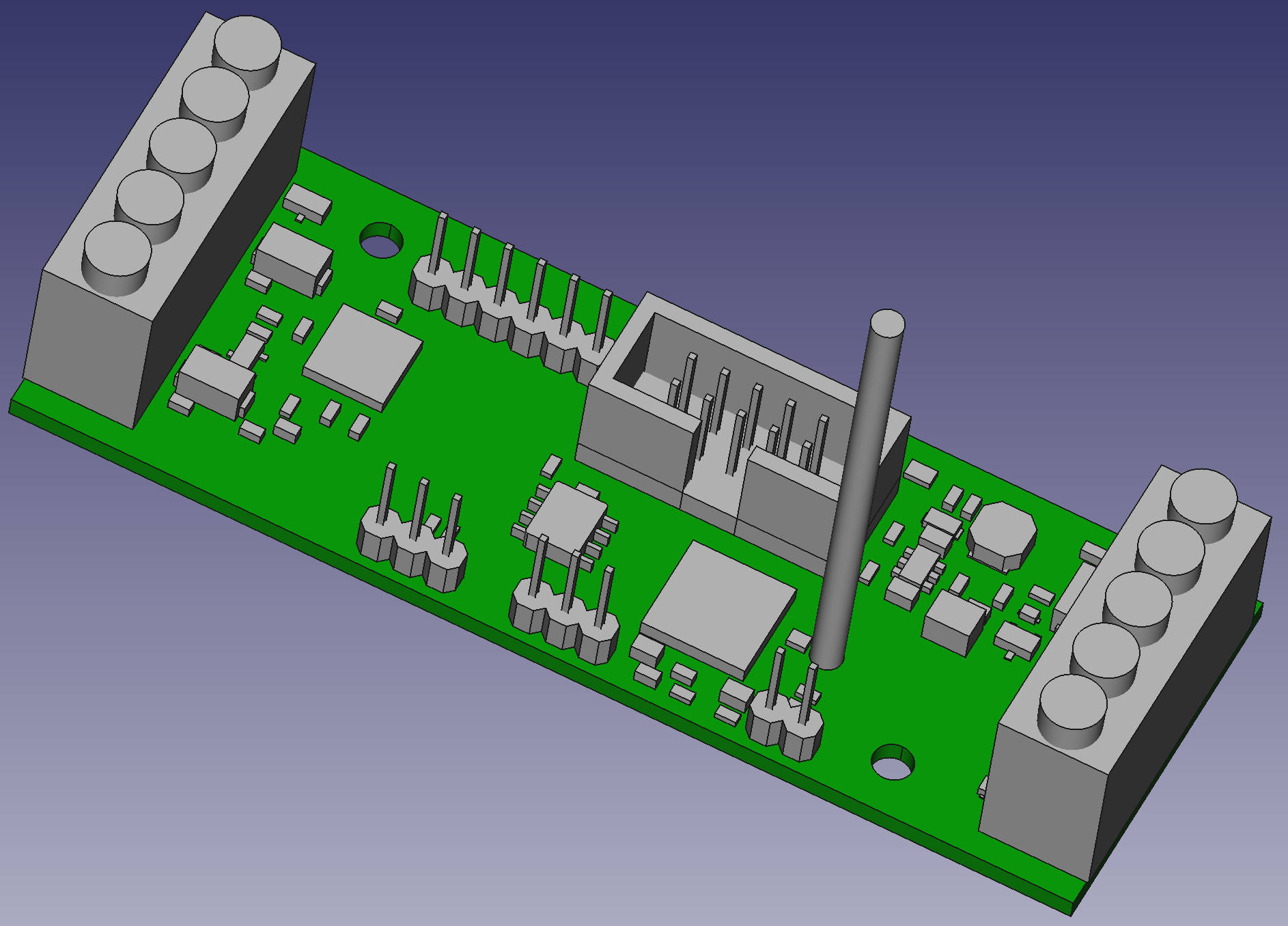
So the Part of the electrical engineer is to generate 3D Data somehow :), which can be used by the mechanical engineer. I am generating STEP Files, which can be viewed with Free STEP Viewers, and integrated by every professional CAD Program.
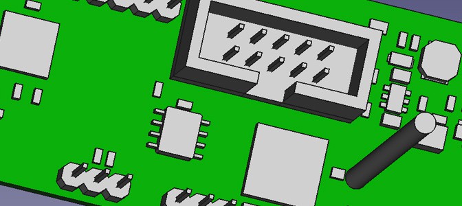
3D Electronic Assembly Model
To generate this type of STEP Data is easy and can be done with EAGLE and a tiny tool, called idfstepper, within seconds. In this Tutorial i will describe this few steps, which are needed to setup all EAGLE part libraries to generate STEP data.
In addition to the main system controller module as described in the post from June 12, i had to design something for me completely new. A RF Module has to be integrated for a Prototype ZWave to Industrial Analog Outupt:
0-10V (default)
0-5V
0-20mA
4-20mA
The ZWave Module is getting values from 0-255 from a ZWave Controller and these Values should be mapped to the DAC output. For this purpose i was going to use a tiny Microchip 8bit MCU (PIC18LF14K22) a DAC from Analog Devices, providing functionalities as described (AD5412) and a ZWave Module (ZM5202) for RF Communications connected via a serial Interface to the MCU. The RF Module has 50Ω Output Impedance, so for optimum RF Performance i had to design a 50Ω trace on the PCB for connecting a Antenna for 868,42 MHz.
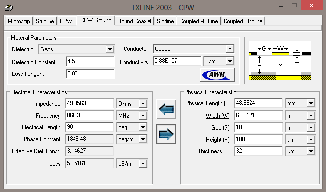
Therefore i took a look into the Design Tool TXLine:
I considered a PCB Anenna Trace in the configuration “Coplanar Waveguide with Ground”. When using standard FR4 PCB Material you are going to expect a Dielectric Constant of 4.3 -4.7 and a Loss tangent of 0.021.
In a Layer Stackup when using 100um Prepreg and a Gap of 10mil im going to expect a Trace Impedance of 49.95Ω. In order to meet the requirements of the PCB Manufacturer i changed the Prepreg Thickness to 360um.
Antenna Trace as CPWG
Therefore the Trace dimensions and the Gap to the Top GND Plane had to be adopted. In order to get best HF-Performance on the PCB it is recommended that you guide the Antenna Trace, not only with the Top GND Plane, you also have to make this GND very “low inductive”. So placing additional GND Via’s near the Trace is a good idea. As it can seen on the picture i added many of them. In fact i never designed impedance controlled traces before, i added a PI Filter Structure for Antenna matching if necessary. First tests were made without any matching circuitry and the RF performance was good. So no further maching was done. During my research i found another useful Tool for designing Impedance controlled traces and differential pairs: Saturn PCB Design ToolKit. Its free, it does a good job and its really easy to use. I really recommend that Tool for every PCB designer to check the Impedance of critical Traces!
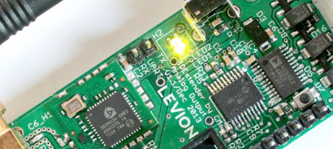
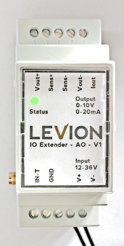
After some startup problems, i was getting better and better in understanding the ZWave Serial API. Coding the firmware for some essential functions (ZWave- inclusion\exclusion, Basic- set\get) was a bit challenging but now it works fine. Acutal the Operating Voltage is polarity protected and any Voltage can be choosen between 10.8V and 36V. When mounted in the housing for DIN Rail mount it looks like this.
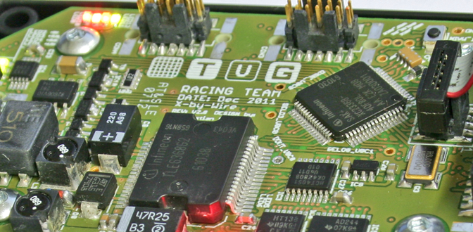
I’m glad to say, that after a few tests nearly the whole hardware on the new board ist fully functional now. The housing with the mounted connectors is also ready now to be put into the car.
A few Softwareupdates should also fit the X-by-Wire System to the Formula Student Electric Rules for 2012.
I expected to finish the whole board weeks ago, but i was busy with several other Projects. For example our Battery Management System – and the Powertrain testbench needed a lot of help, because due to some unecpected issues the installation and build-up was delayed by weeks… However it’s really exciting to see how all Systems in our car are getting more and more functional. Maybe i’ll post some pictures of our High Voltage Containment when it’s build up and give a few explanations how the Battery Management System (short: BMS) works in our car.
