Where PCB Perfection starts – Part1

The CAD Program

There are several tools existing, and many work well. But in my opinion E.A.G.L.E Layout editor is one of the, compared with others, cheapest editors you might can get. If you are only using two layers in Layout and only need euro-card sized PCB’s its free. As far i know most other Editors are organized in a similar way.

The Schematic Editor uses the parts Symbols.
The Layout Editor uses the parts Packages.
The Part Library connects Symbol Pins with physical Package Pins.

One Symbol can be connected to different Packages e.g. one Resistor Symbol can be realized as case size 0603 or 0805 as Package.

In my upcoming posts i will show you some details you have to consider when generating part libraries by your own. I am working with E.A.G.L.E so some tips are only useful if you are using Eagle, but especially for designing Part Libraries on your own, all Information given here might be helpful to you.

How to start your electronic design

When designing Electronic hardware e.g. building a prototype, you might have to design Schematics and Layout by yourself, and if you want to save some money you may also assemble the electronic components on the PCB by yourself.

In this chapter i am going to show up some things that you may have to take into account when building a prototype, also considering some Problems you might do not want to get when looking further to series production.

  1. Component Libraries
  2. Schematic and Layout
  3. Assembly Process (SMT\THT)
  4. Electromagnetic Compatibility (EMC)

On one hand very important is, that the parts you are using can be assembled in a way of your choice. This means you may choose your design rules according to the assembly method. On the other hand when you are designing Schematics and Layout by yourself, you may have to take some standards or regulations into account. EMC is not only a big thing when you want to sell something, it’s also necessary for the whole electronic system to be functional and robust.

I will give you some Guidelines you can follow and also show you how to handle some Problems. These will be shown by time in this blog starting from scratch.

Printing with free solder stencils

As you might have seen already some online PCB manufacturers are providing free stencils. These stencils are a bit larger than your PCB outline dimension will be, but you will need that oversize for your solder paste printer.

Since i was working nearly every day with soldering stencils some years ago i know some tricks to handle the printing process to get optimal results. Let me say, you do not have to be a professional to do this, but there are only a few things in that printing step that have to be considered – and then you will be fine:

  • First of all double check that the stencil fits well, so you do not see any green solder stop mask through the wholes of your stecil (Photos will follow soon).
  • You should be aware of some critical properties of the solder paste:
    • store the paste in the refridgerator in really dry conditions at less than 10°C so you can use the solder paste for a longer time.
    • when printing, take the solder paste half an hour before using out of the refridgerator, so that the paste can get slow up to 22°C room temperature. This is the perfect printing temperature. If its colder the paste wont get through the stencil down to the PCB, if its much more hotter the flux will trickle away when printing, and the prining results wont be stable. After printing put the paste back to the refriderator, unless it will pull water out of the Air in your Lab which will then result in boiling water drops trapped in the solder paste when reflowing in the oven.
    • if you have small pads you may have to use fine pitch solder paste which will have smaller tin balls, than the standard paste.
    • every paste may need other preheat-, soak-, and reflow phase times and temperatures, which have to be considered to get optimum solder results. You will have to check that phase times and temperatures as well as the temperature gradients to fit to your paste. This is in most cases achieved with a thermocouple and a sample PCB Board in the oven to set up the temperature profile according to your solder paste datasheet. Some ICs will also have some reflow requirements but the most restricting part in this phase times is in most cases the solder paste.
  • When printing the paste do not try to pump the paste through the stencil. Take your squeegee in 45° to the the stencil an the move with 1cm/s forward. The paste will fall down through the holes completely without any force from the top side of the stencil with your squeegee. If you push the paste down into the stencil openings the printing result will get worse.

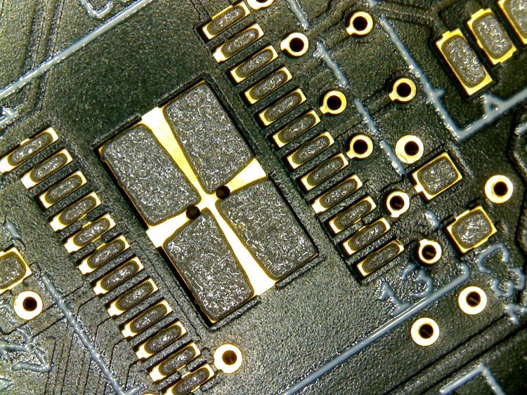
A good printing result, with a free laser stencil and a really cheap printing device can be more or less looking like this:

Solder Paste - free stencil
Printing Results with a free stencil, pad-centered and form-stable print

As a good sample here, you see here, if you have large SMD Pads it is recommended to put air channels into the stecil (mostly a cross form is used), so that the expanding gas – generated by the highly heated flux – can escape from under the Integrated Circuit, so that there are no voids, which you might know are really bad in terms of thermal and electrical conductivity.


How to start electronic Designs? – or what assembly possibilities do i have

In principle i see 3 ways of assembly options for prototypes:

  • manual assembly of all electronic parts without any use of reflow technology
    (cheap and fast but maybe not suitable for all SMT Parts)
  • manual assembly of all electronic parts with partly use of reflow technology
    (relatively cheap and fast but suitable for nearly all SMT Parts)
  • automatic\manual assembly by professional Assembler
    (costly and takes additional 3-5 Weeks, but useful for all SMT Parts)

The first two points are in my opinion, suitable for many designs, where costs really matter, e.g. if you are prototyping something for yourself. Anyway the PCB designer has to consider these points when choosing the electronic components. When looking at my racing team Projects you may have noticed that all PCB’s there were assembled by myself only with one soldering tool. With a ERSA-icon nano and some different tips you can solder nearly everything you can see. There is no Problem with QFP or TSSOP Packages down to 0.5mm pitch. With that solder tool you can do this easily. But, if you have to use an IC which you only get in QFN, any other leadless Chip Carrier Package or BGA, you will have to use a reflow process for assembly.

Small reflow Systems are about 500€ overall costs. You will get good soldering results and you are approximately two times faster than if you only solder all parts by hand. When your designs starting to grow 50+ parts, it really makes sense to use such kits. So these small reflow systems might be the right choice for your project.

“Because of my last soldering results with such a tiny oven and direct comparison to the assembly results with fully manual soldering, this second option from above will really be my favourite choice for assembling homemade-semiprofessional PCBs. It works fine and it saves so much time”

How to set up your assembly process and what design rules you have to keep in mind when doing the Board Design will be shown in the upcoming posts.

Distributed Microcontroller Systems – Delayed

Long Time no see 😉

But a totally new project is upcoming and consuming a lot of time. This project, which is similar to the Distributed Microcontroller Systems Idea, will be in addition used for my telematics semiar project

The only difference for me is, that i’m not goinig into the software part, its more proofing the hardware for satisfying the compliance of EMC/EMI standards. Furthermore some other important points have to be considered when designing PCB’s for series production.

The first prototype boards will arrive at the end of july and they will have the following components on board:

  • Freescale i.MX6 Quadcore CPU (512MB NAND Flash, 4x1GHz) edit: changed to Solo (1x1GHz)
  • WLAN, LAN
  • ZWave Option
  • USB Host
  • USB otg
  • HDMI
  • 7” Display + PCAP Touch

Till now i have designed many boards, but when thinking about the mentioned points this will really not be a simply PCB anymore. Therefore the developer team decided to take advantage from phytec developers, which are more confident with such complex designs, and develop the boards together with them.

So it’s clear, that this is a bit different to the original  Distributed Microcontroller Systems thoughts, but with additional Extensions it will become the more similar to the original idea. If i’m able to post more informations in detail or some pictures i will add it here immediately.

Innovative Electronic Design – pushing the limits