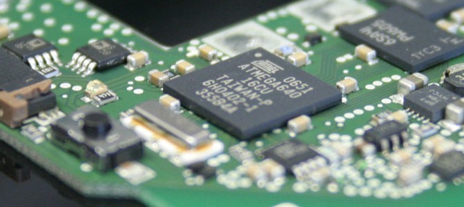
As you might have seen already some online PCB manufacturers are providing free stencils. These stencils are a bit larger than your PCB outline dimension will be, but you will need that oversize for your solder paste printer.
Since i was working nearly every day with soldering stencils some years ago i know some tricks to handle the printing process to get optimal results. Let me say, you do not have to be a professional to do this, but there are only a few things in that printing step that have to be considered – and then you will be fine:
- First of all double check that the stencil fits well, so you do not see any green solder stop mask through the wholes of your stecil (Photos will follow soon).
- You should be aware of some critical properties of the solder paste:
- store the paste in the refridgerator in really dry conditions at less than 10°C so you can use the solder paste for a longer time.
- when printing, take the solder paste half an hour before using out of the refridgerator, so that the paste can get slow up to 22°C room temperature. This is the perfect printing temperature. If its colder the paste wont get through the stencil down to the PCB, if its much more hotter the flux will trickle away when printing, and the prining results wont be stable. After printing put the paste back to the refriderator, unless it will pull water out of the Air in your Lab which will then result in boiling water drops trapped in the solder paste when reflowing in the oven.
- if you have small pads you may have to use fine pitch solder paste which will have smaller tin balls, than the standard paste.
- every paste may need other preheat-, soak-, and reflow phase times and temperatures, which have to be considered to get optimum solder results. You will have to check that phase times and temperatures as well as the temperature gradients to fit to your paste. This is in most cases achieved with a thermocouple and a sample PCB Board in the oven to set up the temperature profile according to your solder paste datasheet. Some ICs will also have some reflow requirements but the most restricting part in this phase times is in most cases the solder paste.
- When printing the paste do not try to pump the paste through the stencil. Take your squeegee in 45° to the the stencil an the move with 1cm/s forward. The paste will fall down through the holes completely without any force from the top side of the stencil with your squeegee. If you push the paste down into the stencil openings the printing result will get worse.
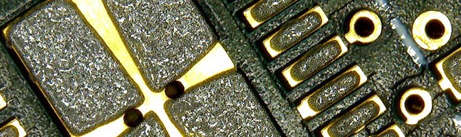
A good printing result, with a free laser stencil and a really cheap printing device can be more or less looking like this:
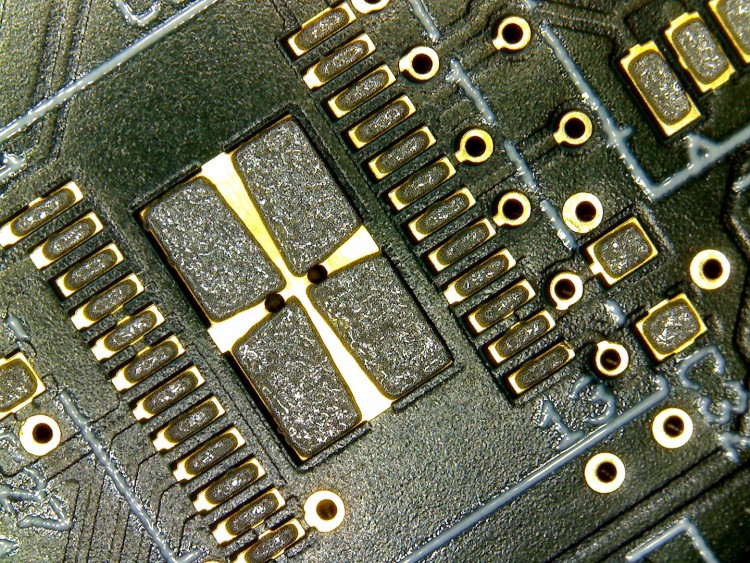
As a good sample here, you see here, if you have large SMD Pads it is recommended to put air channels into the stecil (mostly a cross form is used), so that the expanding gas – generated by the highly heated flux – can escape from under the Integrated Circuit, so that there are no voids, which you might know are really bad in terms of thermal and electrical conductivity.