When designing Electronic hardware e.g. building a prototype, you might have to design Schematics and Layout by yourself, and if you want to save some money you may also assemble the electronic components on the PCB by yourself.
In this chapter i am going to show up some things that you may have to take into account when building a prototype, alsoconsidering some Problems you might do not want to get when looking further to series production.
On one hand very important is, that the parts you are using can be assembled in a way of your choice. This means you may choose your design rules according to the assembly method. On the other hand when you are designing Schematics and Layout by yourself, you may have to take some standards or regulations into account. EMC is not only a big thing when you want to sell something, it’s also necessary for the whole electronic system to be functional and robust.
I will give you some Guidelines you can follow and also show you how to handle some Problems. These will be shown by time in this blog starting from scratch.
If you have a part symbol and package set up properly you can go on with setting up a new device and the devices technologies.
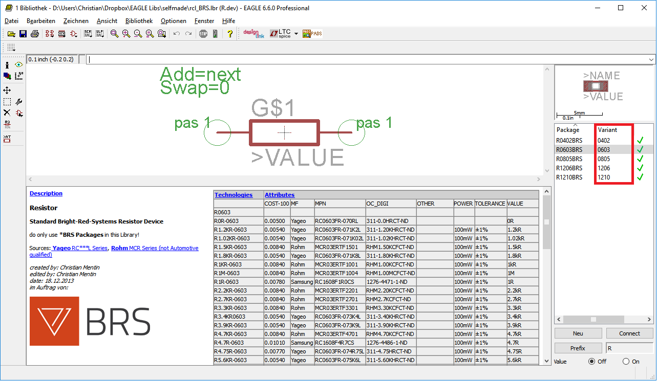
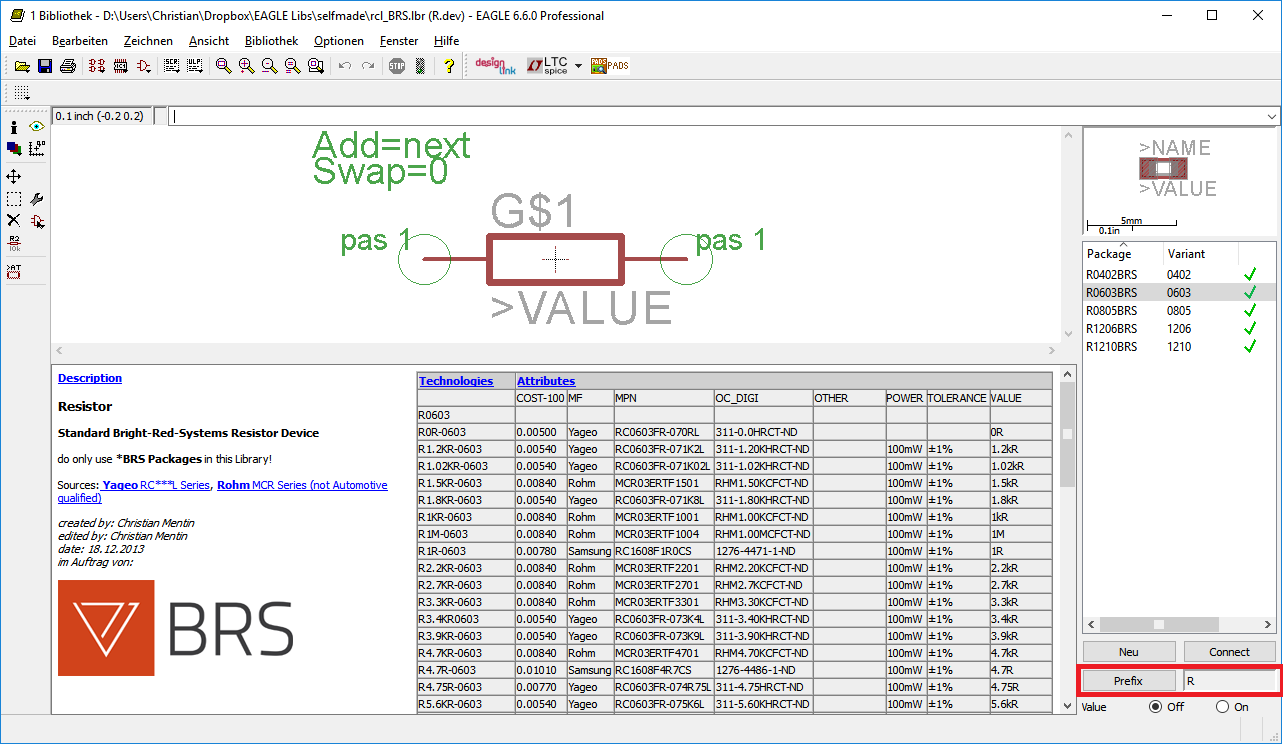
In the Device Editor you have to create a new Device and add a Symbol (by simply). To have an easy example we will start with an simple 2 terminal resistor, and call the device R. Then you add your Package Variants, as i did here. I’ve added some Packages i have drawn before, and connect Symbol Pins with the Package Pins.
The Package Variant Name will be directly shown in the Technology Name, therefore i named the Variants in my example 0603, 0805 and so on.
The Prefix of the Device will be Name of the Part in the Schematic trailed by a ongoing unique Number. Here it will be starting with R1, R2 etc.
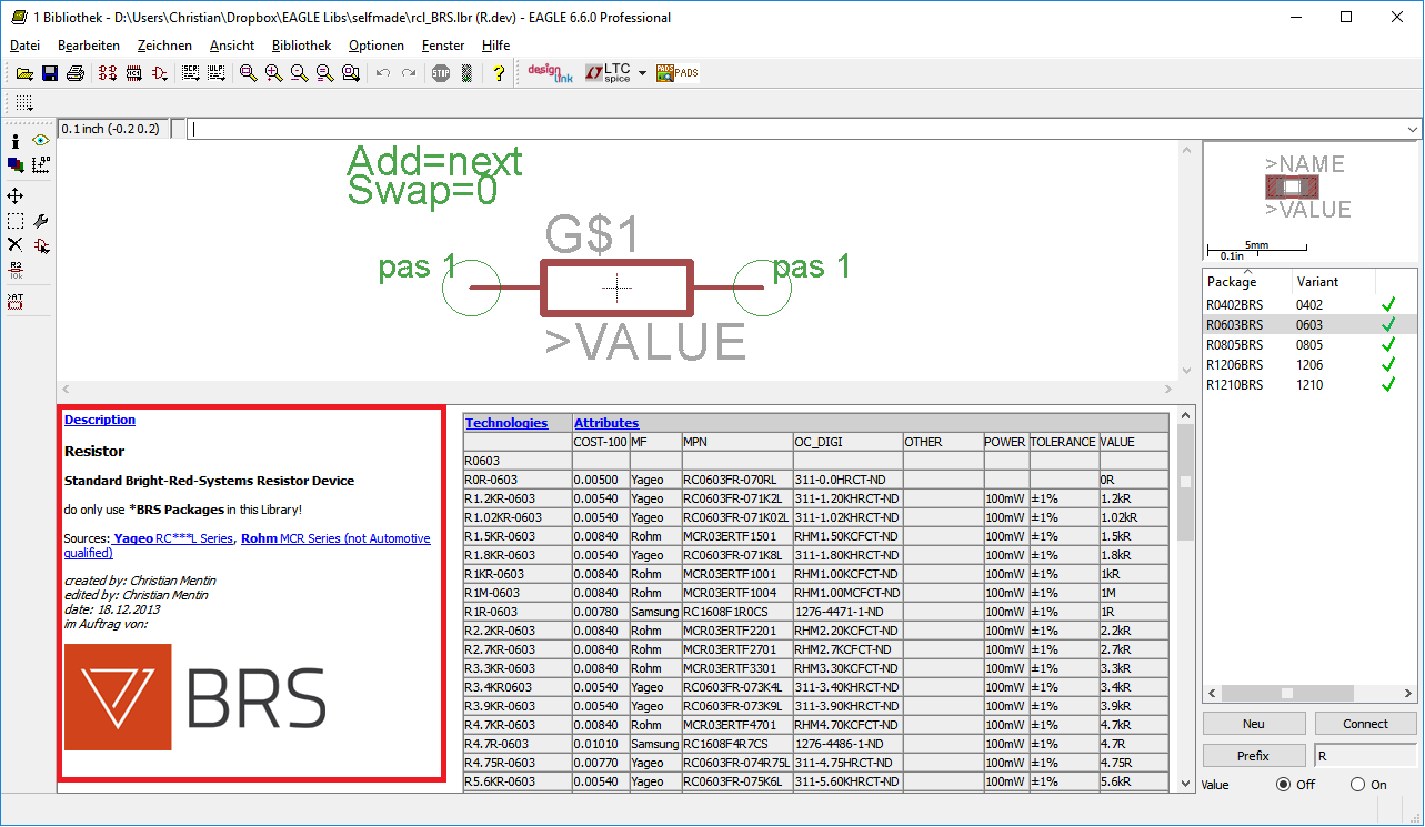
The Description can contain html formatted Information, and is useful for containing links to Datasheets of used Parts in the technologies.
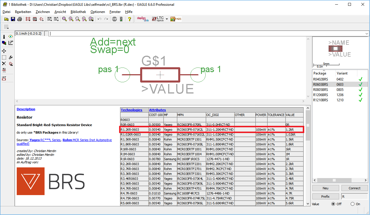
And at last the most important, creating technologies. Every Package Variant can have several Technologies.
For example think of a 0603 Resistor, in values 1kOhm and 100kOhm. These would be the Technologies (i created here some more technologies for later use) in the Package Variant 0603. After adding these technologies you can easily add attributes and fill in the Information for every technology and every attribute. If you include an attribute called Value, the placed technology would automatically set this value for the part in schematic and layout editor.
Some Attributes which should always be added for a complete BOM export: MF (Manufacturer) MPN (Manufacturer Part Number) OC (Order Code) OTHER (for some additional Information) VALUE (for the displayed Value)
additional Attributes for faster part choice which i use in some other devices could be:
POWER (rated Power)
TOLERANCE (Tolerance in Value)
COST-100 (cost of 100Parts@supplier)
I-SAT (saturation current of a coil)
RDC (DC Resistance of e.g. a coil)
IDC_MAX (maximum DC Current)
VOLTAGE (rated Voltage e.g. of a Capacitor)
If you keep all that in mind when creating a new Device you will get a sweet Bill of Materials with every Information you need with one easy click. To see such a sample BOM only created by filling in all listed attributes in every device you will get something like this:
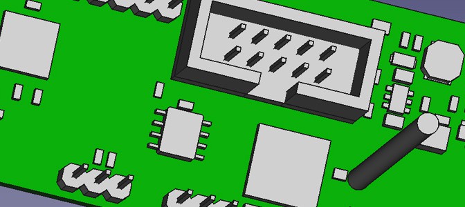
Every electronic designer may need a simple mechanical integration into a housing or only some protective shields for his electronic assembly.
In my opinion the most critical point is, when some connectors have to be soldered directly onto the PCB or if they are mounted into the case walls and reaching far into the housing. In this case, some simple 3D PCB Information is sufficient to see if there are collisions, and if the whole assembly group fits into the housing. Well, this check may be part of the mechanical designer, but to ease this step 3D PCB Data is required.
So the Part of the electrical engineer is to generate 3D Data somehow :), which can be used by the mechanical engineer. I am generating STEP Files, which can be viewed with Free STEP Viewers, and integrated by every professional CAD Program.
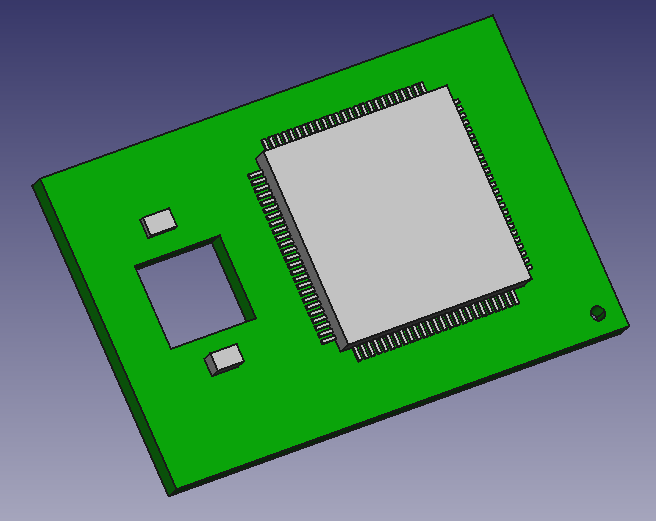
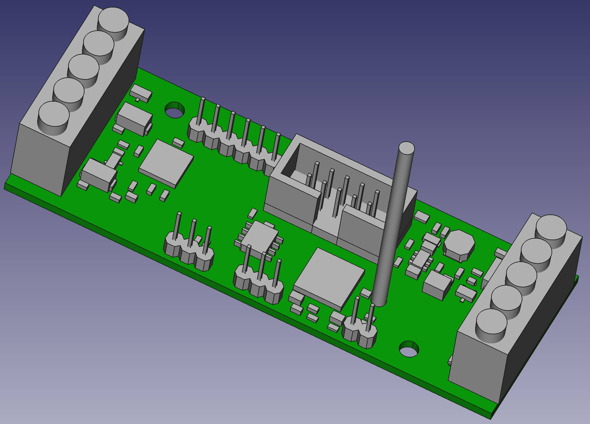
3D Electronic Assembly Model
To generate this type of STEP Data is easy and can be done with EAGLE and a tiny tool, called idfstepper, within seconds. In this Tutorial i will describe this few steps, which are needed to setup all EAGLE part libraries to generate STEP data.
The Symbol, displaed in the Schematic Editor The Package, displayed in the Layout Editor The Device, connects Symbol- with Package pins
What you really should consider is to use device technologies. This will enable you the power of one-click generation of your Bill of Materials (BOM), with all Part Numbers and Distributor Order Codes, of every Part you used in your Design. To benefit of this BOM Generation, since Ealge6 its directly located under
file->export, it is recommended to use device technologies, for every single Part!
At the first look it seems that this might be some horrible work, but its only the very first time. Once you have device technologies, for every part (resistors, capacitors etc.) schematic design with choosing all parts, will be very very easy, because you wont have to look up order codes never ever again.
Ordering Parts at your Distributor for a whole Project will be done in one minute with a simple copy paste of your BOM.
In the next Tutorial i will show you how to set up a Device and the technologies in a professional way.
FreeCAD – for viewing generated 3D Data and assembly with housing models.
If you are using EAGLE, you know how libraries are organized in Symbols, Packages and Devices.
In some other tutorials i will show how to set up all library Informations properly, this tutorial will focus only on the library parts concerning 3D Data, which is the Package Information. This additional Infomation to generate step-files will cost you maybe one additional minute when creating a new Package but the 3D Information you get is completely amazing.
First of all you will have to generate some new layers in the Package of a Device:
PackageLayer 57: for top placed parts
PackageLayer 58: for bottom placed parts
(just copy paste into the command line of eagle-Package Editor: layer ’57’ tCAD or layer ’58’ bCAD)
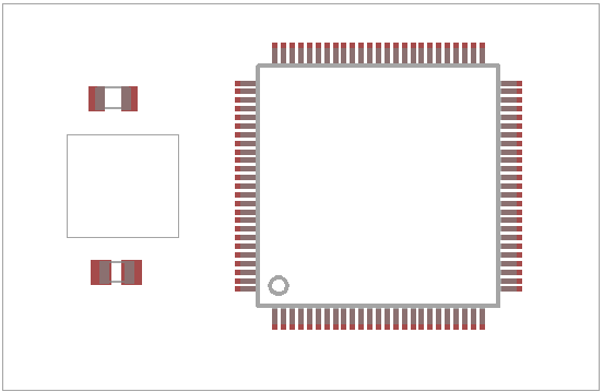
By only drawing the outlines of your part in this layers, shapes will later be extruded with the height of your line width (1 µm width = 1mm heigth). The line width determines the extrusion height. If you want some pins of your e.g. TQFP part shown in the 3D Model you will have to draw extra rectangular shapes for every pin.
Layer 57: tCAD Polygons for Plastic Case and Pins
Be aware, that eagle connects lines which are close together, to a single polygon, therefore, parallel outline shape of pins and plastic case should not be connected since you will get errors when generating the idf-file. You can check if they are connected, by zooming in wide, or only moving the shapes a bit. You will see if they stick together immediately. To have no problems i move the conours by entering the numbers directly into the Info of a shape contour, so they will always be in a distance of more than 1µm. In the 3D Model you wont see that distance between feet and plastic case.
NOTE: Be sure that you draw something like the maximum outline dimensions, since big parts may have mm Tolerances and they might collide in your housing if you don’t consider that sometimes parts are bigger than the typ. size shown in the Datasheets!
Layer 50: PCB Outline with PCB cutout
Next step is to generate a new layer in your .brd: .brdLayer 50: for the PCB Outline (you may copy only the Dimension to that Layer). as in the Package.
The line width also determines the PCB Thickness, in the same way.
one simple PCB Outline with a breakthrough and three simple Parts placed
If you want some cutouts or breaktroughs in your Board, you can do so by defining a Polygon with line width set to 0.0µm. When you are done with the Layout, here in my tiny example i only put one Resistor and another Capacitor onto the Board, it may look something like this.
After that you will have to generate the 3D idf Data with a eagle ulp Program called generate-3d-idf-data.ulp.
step file generated with idf-stepper (idf and idb file as Input)
There will be 2 files generated. On is the named *.idf and it contains the information of the whole polygons. idf-stepper will generate a step file for every single polygon and store it in the root folder. The *.idb file contains the Information how the polygons are oriented to the Board origin. idf-stepper will take all the generated step files, put them in place to one big step assembly. In windows idf-stepper works with drag&drop the *.idf and *.idb files simply onto the executable and you are done!
When you are using your simple rectangular shapes like me in my little example you will then get a generated step file looking something like this. For most Mechanical Engineers this generated step Information is all what they need to place the parts in a mechanical assemly and check collisions and correctness of mounting points.
But idf-stepper also can also deal with advanced very complex step models. Exactly this function gives you the most powerful capability:
By only using the *.idb file you can take every very advanced 3D Model as Input source to the idf stepper. Only take a short look at the naming convention, take your advanced model, give it the right orientation and you can use it immediately by replacing the generated step file of this part generated by idf-stepper. If you deliver the idf-stepper only the *.idb file as Input, the existing step files wont be overwritten.
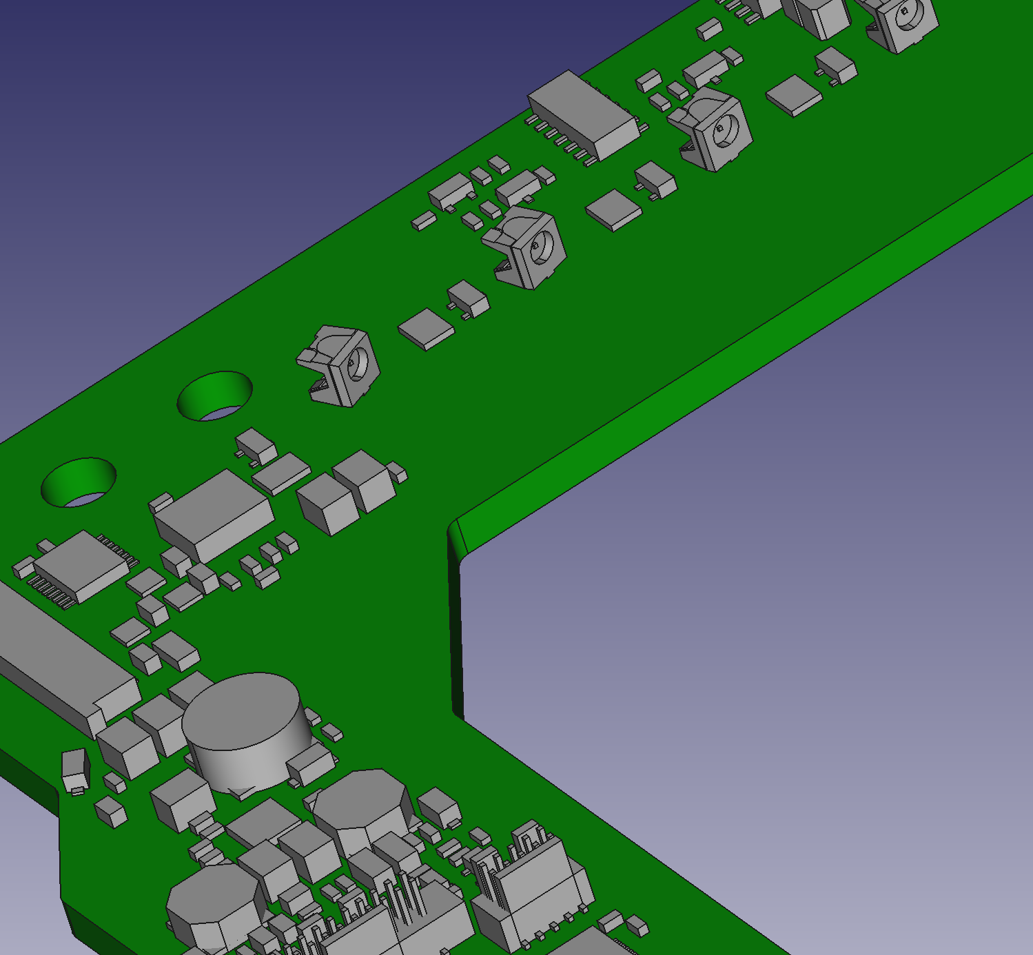
In another Project i used more advanced 3D Models for the LEDs, once you have rotated the advanded LED-Models into the right angles, you can use them every time again:
included advanced step files for LEDs
One addiotional highly useful and powerful feature: Since FreeCAD has the Ability to save the step file as *.html (every modern Browser can use WebGL) you can send your 3D Model as html-file to everyone, still if he has no CAD Viewer, he will be able to rotate the model, zoom in/out within the browser. The only thing you might have to adjust by your own with a simple text editor is, to set the camera Position far enough from your board, since if the standard Position is (0.0, 0.0, 1.0), which means the camera is set in the PCB, so by default you do not see any parts. I like to use something like that camera.position.set( 100.0, 100.0, 200.0 );
This last sample i provided here, outgoing from an with idf-stepper generated step-file, opened with FreeCAD and saved as html(webGL) file.
Most electronic desings start with the schematic editor, placing some parts and changing their values. Not every designer is thinking about concrete parts (Manufacturer Product Number – MPN), their physical case dimensions, and the availability when designing the schematic.
What you really have to consider is, what component technologies you might want to use, in order to meet your assembly requirements. Threrefore you might have to look for TSSOP Cases instead of no-leaded QFN packages. Most active parts you will get in different cases directly from the distributor, only take a look into the Datasheet, all possible packages of one part are clearly shown, often with dimensions and order codes (Maufacturer Part Number). As an Exaple you might take a look into that Datasheet of a DAC. You could freely choose between TSSOP or QFN Package, the costs and the availability at the distributor is nearly the same.
When using parts in the schematic it makes clearly sense to think about what concrete part, also what passive components like resistors and capacitors, you will place in your layout, especially if some cases may have long lead times.
So when you already know what parts you want to use its time to set up your CAD Library properly.
![[Tutorial] Generating 3D PCB Data in seconds](https://blog.mentin.at/wp-content/uploads/CCarrier_3D_featured_1038px-2-672x300.jpg)